/blog/post/1729028In the above reply I describe the difference between a Thyristor(GTO i.e Gate Turn Off Thyristor) and Transistor(IGBT i.e Insulated Gated Bi-Polar Transistor)
Now in both of the above references one thing is Common that both GTO & IGBT are "SEMICONDUCTOR DEVICE" used in 3-Phase Locomotives. In perspective of this line it is now very Imperative to share the knowledge of "Semiconductor Device" in details here. So that all of you can know the Concept of "Semiconductor Device" in details.
Semiconductor Device:
Semiconductor devices are electronic components that exploit the electronic properties of semiconductor materials, principally silicon, germanium, and gallium arsenide, as well as organic semiconductors. Semiconductor devices have replaced thermionic devices (vacuum tubes) in most applications. They use electronic conduction in the solid state as opposed to the gaseous state or thermionic emission in a high vacuum.Semiconductor devices are manufactured both as single discrete devices and as integrated circuits (ICs), which consist of a number—from a few (as low as two) to billions—of devices manufactured and interconnected on a single semiconductor substrate, or wafer.Semiconductor materials are useful because their behavior can be easily manipulated by the addition of impurities, known as doping. Semiconductor conductivity can be controlled by introduction of an electric or magnetic field, by exposure to light or heat, or by mechanical deformation of a doped monocrystalline grid; thus, semiconductors can make excellent sensors. Current conduction in a semiconductor occurs via mobile or "free" electrons and holes, collectively known as charge carriers. Doping a semiconductor such as silicon with a small amount of impurity atoms, such as phosphorus or boron, greatly increases the number of free electrons or holes within the semiconductor. When a doped semiconductor contains excess holes it is called "p-type", and when it contains excess free electrons it is known as "n-type", where p (positive for holes) or n (negative for electrons) is the sign of the charge of the majority mobile charge carriers. The semiconductor material used in devices is doped under highly controlled conditions in a fabrication facility, or fab, to control precisely the location and concentration of p- and n-type dopants. The junctions which form where n-type and p-type semiconductors join together are called p–n junctions.
For more details and various Types of Semiconductor Device please refer:
click hereWhat is p-nJunctions in c/w with Semiconductors?
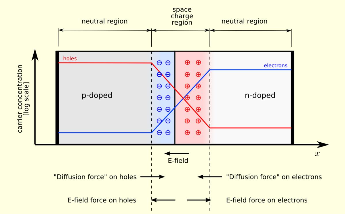
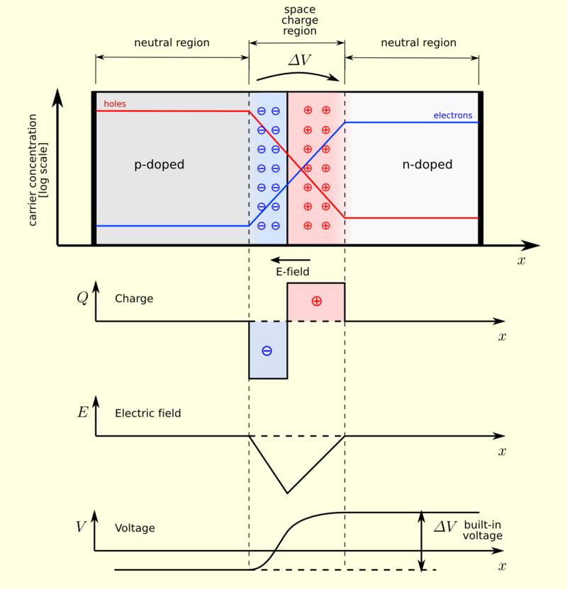
Ans: A p–n junction is a boundary or interface between two types of semiconductor material, p-type and n-type, inside a single crystal of semiconductor. It is created by doping, for example by ion implantation, diffusion of dopants, or by epitaxy (growing a layer of crystal doped with one type of dopant on top of a layer of crystal doped with another type of dopant). If two separate pieces of material were used, this would introduce a grain boundary between the semiconductors that would severely inhibit its utility by scattering the electrons and holes.p–n junctions are elementary "building blocks" of most semiconductor electronic devices such as diodes, transistors, solar cells, LEDs, and integrated circuits; they are the active sites where the electronic action of the device takes place. For example, a common type of transistor, the bipolar junction transistor, consists of two p–n junctions in series, in the form n–p–n or p–n–p.The discovery of the p–n junction is usually attributed to American physicist Russell Ohl of Bell Laboratories.However, Vadim Lashkaryov reported discovery of p-n-junctions in Cu_2O and silver sulphide photocells and selenium rectifiers in 1941.A Schottky junction is a special case of a p–n junction, where metal serves the role of the p-type semiconductor.
For more details on p-njunction please refer:
click hereWhat is p-type and n-type semiconductor material ?(Also known as Extrinsic Semiconductor)
Ans:
click hereWhat is "Doping Agent/Dopant" used in Extrinsic Semiconductor ?
Ans:
click hereAttached Images:
An n–p–n bipolar junction transistor structure
Link:
click herePn-junction-equilibrium
Link:
click herePn-junction-equilibrium-graphs
Link:
click here(Hope from this BLOG all of you get a Complete Idea about Semiconductors used in 3-Phase Loco[i.e WAP-5/WAP-7 & WAG-9] of Indian Railways)